- 您现在的位置:买卖IC网 > Sheet目录2002 > KAD5512HP-17Q72 (Intersil)IC ADC 12BIT 170MSPS SGL 72-QFN
9
FN6808.3
October 1, 2009
Pinout/Package Information
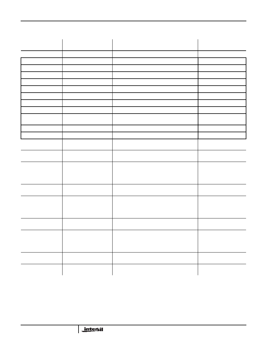
Pin Descriptions - 72QFN
PIN NUMBER
LVDS [LVCMOS] NAME
LVDS [LVCMOS] FUNCTION
SDR MODE
DDR MODE COMMENTS
1, 6, 12, 19, 24, 71
AVDD
1.8V Analog Supply
2-5, 13, 14, 17, 18, 28-31
DNC
Do Not Connect
7, 8, 11, 72
AVSS
Analog Ground
9, 10
VINN, VINP
Analog Input Negative, Positive
15
VCM
Common Mode Output
16
CLKDIV
Clock Divider Control
20, 21
CLKP, CLKN
Clock Input True, Complement
22
OUTMODE
Output Mode (LVDS, LVCMOS)
23
NAPSLP
Power Control (Nap, Sleep modes)
25
RESETN
Power On Reset (Active Low, see “User-Initiated
26, 45, 55, 65
OVSS
Output Ground
27, 36, 56
OVDD
1.8V Output Supply
32
D0N
[NC]
LVDS Bit 0 (LSB) Output Complement
[NC in LVCMOS]
DDR Logical Bits 1, 0 (LVDS)
33
D0P
[D0]
LVDS Bit 0 (LSB) Output True
[LVCMOS Bit 0]
DDR Logical Bits 1, 0 (LVDS
or CMOS)
34
D1N
[NC]
LVDS Bit 1 Output Complement
[NC in LVCMOS]
NC in DDR
35
D1P
[D1]
LVDS Bit 1 Output True
[LVCMOS Bit 1]
NC in DDR
37
D2N
[NC]
LVDS Bit 2 Output Complement
[NC in LVCMOS]
DDR Logical Bits 3,2 (LVDS)
38
D2P
[D2]
LVDS Bit 2 Output True
[LVCMOS Bit 2]
DDR Logical Bits 3,2 (LVDS
or CMOS)
39
D3N
[NC]
LVDS Bit 3 Output Complement
[NC in LVCMOS]
NC in DDR
40
D3P
[D3]
LVDS Bit 3 Output True
[LVCMOS Bit 3]
NC in DDR
41
D4N
[NC]
LVDS Bit 4 Output Complement
[NC in LVCMOS]
DDR Logical Bits 5,4 (LVDS)
42
D4P
[D4]
LVDS Bit 4 Output True
[LVCMOS Bit 4]
DDR Logical Bits 5,4 (LVDS
or CMOS)
43
D5N
[NC]
LVDS Bit 5 Output Complement
[NC in LVCMOS]
NC in DDR
44
D5P
[D5]
LVDS Bit 5 Output True
[LVCMOS Bit 5]
NC in DDR
KAD5512HP
发布紧急采购,3分钟左右您将得到回复。
相关PDF资料
KAD5512P-17Q72
IC ADC 12BIT 170MSPS SGL 72-QFN
KAD5514P-12Q72
IC ADC 14BIT 125MSPS SGL 72-QFN
KAD5610P-25Q72
IC ADC 10BIT 250MSPS DUAL 72-QFN
KAD5612P-17Q72
IC ADC 12BIT 170MSPS DUAL 72-QFN
LA72715NV-TLM-E
IC AUDIO DECODER JPN MTS 24SSOP
LICAL-DEC-LS001
IC DECODER LOW SECURITY 8DIP
LICAL-DEC-MS001
IC DECODER MS SERIES 20-SSOP
LICAL-ENC-MS001
IC ENCODER MS SERIES 20-SSOP
相关代理商/技术参数
KAD5512HP-21Q48
功能描述:模数转换器 - ADC 12-BIT 210MSPS HI PERF SINGLE ADC PROG
RoHS:否 制造商:Texas Instruments 通道数量:2 结构:Sigma-Delta 转换速率:125 SPs to 8 KSPs 分辨率:24 bit 输入类型:Differential 信噪比:107 dB 接口类型:SPI 工作电源电压:1.7 V to 3.6 V, 2.7 V to 5.25 V 最大工作温度:+ 85 C 安装风格:SMD/SMT 封装 / 箱体:VQFN-32
KAD5512HP-21Q72
功能描述:模数转换器 - ADC 12-BIT 210MSPS HI PERF SINGLE ADC PROG
RoHS:否 制造商:Texas Instruments 通道数量:2 结构:Sigma-Delta 转换速率:125 SPs to 8 KSPs 分辨率:24 bit 输入类型:Differential 信噪比:107 dB 接口类型:SPI 工作电源电压:1.7 V to 3.6 V, 2.7 V to 5.25 V 最大工作温度:+ 85 C 安装风格:SMD/SMT 封装 / 箱体:VQFN-32
KAD5512HP-25Q48
功能描述:模数转换器 - ADC 12-BIT 250MSPS HI PERF SINGLE ADC
RoHS:否 制造商:Texas Instruments 通道数量:2 结构:Sigma-Delta 转换速率:125 SPs to 8 KSPs 分辨率:24 bit 输入类型:Differential 信噪比:107 dB 接口类型:SPI 工作电源电压:1.7 V to 3.6 V, 2.7 V to 5.25 V 最大工作温度:+ 85 C 安装风格:SMD/SMT 封装 / 箱体:VQFN-32
KAD5512HP-25Q72
功能描述:模数转换器 - ADC 12-BIT 250MSPS HI PERF SINGLE ADC
RoHS:否 制造商:Texas Instruments 通道数量:2 结构:Sigma-Delta 转换速率:125 SPs to 8 KSPs 分辨率:24 bit 输入类型:Differential 信噪比:107 dB 接口类型:SPI 工作电源电压:1.7 V to 3.6 V, 2.7 V to 5.25 V 最大工作温度:+ 85 C 安装风格:SMD/SMT 封装 / 箱体:VQFN-32
KAD5512P
制造商:INTERSIL 制造商全称:Intersil Corporation 功能描述:Low Power 12-Bit, 250/210/170/125MSPS ADC
KAD5512P_09
制造商:INTERSIL 制造商全称:Intersil Corporation 功能描述:Low Power 12-Bit, 250/210/170/125MSPS ADC
KAD5512P-12Q48
功能描述:模数转换器 - ADC 12-BIT 125MSPS SINGL ADC PROG LVDS/LVCMOS RoHS:否 制造商:Texas Instruments 通道数量:2 结构:Sigma-Delta 转换速率:125 SPs to 8 KSPs 分辨率:24 bit 输入类型:Differential 信噪比:107 dB 接口类型:SPI 工作电源电压:1.7 V to 3.6 V, 2.7 V to 5.25 V 最大工作温度:+ 85 C 安装风格:SMD/SMT 封装 / 箱体:VQFN-32
KAD5512P-12Q72
功能描述:模数转换器 - ADC 12-BIT 125MSPS SINGL ADC PROG LVDS/LVCMOS RoHS:否 制造商:Texas Instruments 通道数量:2 结构:Sigma-Delta 转换速率:125 SPs to 8 KSPs 分辨率:24 bit 输入类型:Differential 信噪比:107 dB 接口类型:SPI 工作电源电压:1.7 V to 3.6 V, 2.7 V to 5.25 V 最大工作温度:+ 85 C 安装风格:SMD/SMT 封装 / 箱体:VQFN-32